Make your own board
Once you have been playing with Arduinos for a while you probably are thinking that you want to deploy one, but without the expense, and physical size, of using a whole new Uno board. This post describes how to do that.
AtMega328P chip
We will start off with a "raw" Atmega328P-PU chip, the sort of thing you might buy off the shelf from Digi-Key, Element14, or other suppliers:

Note that pin 1 is at the end where there is a notch in the plastic and an extra hole on the top.
The chip itself can be purchased for around $US 3.
Anti-static precautions
To avoid "zapping" your chip avoid handling it by the legs. I sit down at a bench, and use long-nosed insulated pliers to hold the chip by the plastic part, not the legs, to avoid destroying it with a static charge.
Minimal wiring
The chip pinouts are:

The very basics are to wire +5V to VCC and AVCC (AVCC is the analog power in), plus both GND pins (normal and analog).
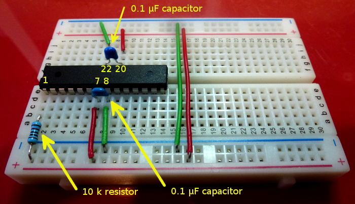
Connected are:
- +5V to VCC (pin 7) (red wire)
- GND to pin 8 (green wire)
- +5V to AVCC (pin 20) (red wire)
- GND to pin 22 (green wire)
- Connect /RESET (pin 1) to +5V via a 10 k pull-up resistor
We also add a 0.1 uF decoupling capacitor on both sides, between VCC and Gnd, and AVCC and Gnd. Note that subsequent photos in this thread show an earlier version of the board with the decoupling capacitors further away, and the green wires as blue wires. It is better to have the capacitors right next to the chip pins.
There is also a 10 k pull-up resistor for the reset pin. Although the chip has a built-in pull-up, this appears to make it reset more reliably when downloading new programs.
There are wire links connecting the Gnd and +5 V of both sides of the breadboard together.
Power supply
The chip requires around +5V power to run. It has an absolute maximum rating of 5.5V, and a minimum of 1.8V. At lower voltages not all clock speeds are available.
For running at 16 MHz you need at least 3.78V and at 8 MHz you need at least 2.40V. (Caveat: under testing I found that it did not seem to work reliably much under 2.8V at 8 MHz).
[EDIT] That unreliability would have been because of the brown-out reset kicking in at 2.7V. If you are using lower voltages you need to adjust or disable the brown-out detection.
I am planning to run at 8 MHz using the internal oscillator, to save parts and space. Thus you could conceivably run the whole thing off 2 x 1.5V batteries, giving around 3V nominally. However 3 x 1.5V batteries would be OK, and let you run it at 16 MHz.
For now, I'll just grab power from the Uno board, while programming it, or from the FTDI connector.
Test the chip
Our next major stage is to upload a bootloader onto the chip. The bootloader simplifies subsequent programming, as it accepts programming commands from the serial port. However we need another chip that supports SPI to burn the bootloader.
So at this stage we need another board, such as a Uno, Duemilanove or so on. Now this is a bit of a "chicken and egg" situation, which is why this process is called "booting".
http://en.wikipedia.org/wiki/Bootstrapping
Grab a second board (which already has the bootloader on it) and connect up 6 wires as shown:

Wiring
Programming Uno     Target board

D10 (SS)            Reset - pin 1 (green)
D11 (MOSI)          Pin 17 (white)
D12 (MISO)          Pin 18 (orange)
D13 (SCK)           Pin 19 (black)

Gnd                 Gnd (blue)
+5V                 +5V (red)
Now grab the "board detector" sketch from here:
https://github.com/nickgammon/arduino_sketches
This particular sketch is in the "Atmega_Board_Detector" subdirectory.
Unzip and upload that into your Uno.
When you run it you should see something like this in the Serial Monitor:
Board Detector Output
Atmega chip detector.
Entered programming mode OK.
Signature = 1E 95 0F
Processor = ATmega328P
Flash memory size = 32768
LFuse = E2
HFuse = DA
EFuse = FD
Lock byte = EF
Bootloader in use: Yes
EEPROM preserved through erase: No
Watchdog timer always on: No
Bootloader is 2048 bytes starting at 7800

Bootloader:

7800: 0C 94 34 3C 0C 94 51 3C 0C 94 51 3C 0C 94 51 3C
...
7FF0: FF FF FF FF FF FF FF FF FF FF FF FF FF FF FF FF

MD5 sum of bootloader = 27 EB 87 14 5D 45 D4 D8 41 44 52 CE 0A 2B 8C 5F

First 256 bytes of program memory:

0: FF FF FF FF FF FF FF FF FF FF FF FF FF FF FF FF
...
F0: FF FF FF FF FF FF FF FF FF FF FF FF FF FF FF FF
Make sure you have the serial monitor baud rate set to 115200 (bottom RH corner).
Your figures may vary a bit but you should certainly see the lines in bold which indicate it detected the chip type.
If you see this, you can skip down to the section "Programming the Bootloader".
If not, read on ...
Chip not detected
If, instead of the above, you see this:
Board Detector Output
This means that the target board has not entered programming mode.
First, double-check your wiring.
If you are certain that is correct, then your target chip is probably configured to need a crystal. The crystal generates the processor clock, and without it you cannot program it.
If you bought a "raw" chip direct from the manufacturer you should not have this problem, as the chips default to using an internal 8 MHz oscillator. But if you got your chip from a third party who already installed a bootloader, then the "fuse settings" may have been changed to expect the crystal.
So, we'll have to install one, or we can't program it.
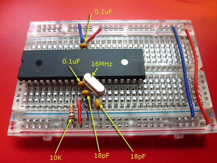
The exact frequency of crystal isn't critical, probably something between 4 MHz and 20 MHz would do, enough to get the processor to start up.
Install the legs of the crystal so they connect to pins 9 and 10 as shown:

Also connect a 22 pF or thereabouts (eg. 18 pF or 20 pF) capacitor between each leg and ground, as shown.
Another angle:

In my case I used an 8 MHz crystal.
An alternative is to use a "resonator" which is similar in behaviour to a crystal, and does not require capacitors:

Connect the outside legs of the resonator to pins 9 and 10, and the middle leg to ground.
With the crystal in place I can now check this chip:
Board Detector Output
Atmega chip detector.
Entered programming mode OK.
Signature = 1E 95 0F
Processor = ATmega328P
Flash memory size = 32768
LFuse = FF
HFuse = DA
EFuse = FD
Lock byte = FF
Bootloader in use: Yes
EEPROM preserved through erase: No
Watchdog timer always on: No
Bootloader is 2048 bytes starting at 7800

Bootloader:

7800: FF FF FF FF FF FF FF FF FF FF FF FF FF FF FF FF
7810: FF FF FF FF FF FF FF FF FF FF FF FF FF FF FF FF
...
7FE0: FF FF FF FF FF FF FF FF FF FF FF FF FF FF FF FF
7FF0: FF FF FF FF FF FF FF FF FF FF FF FF FF FF FF FF

MD5 sum of bootloader = E0 DE EB D3 C3 F5 60 21 2A F1 7C 68 B9 34 4B AE

First 256 bytes of program memory:

0: 0C 94 34 00 0C 94 51 00 0C 94 51 00 0C 94 51 00
10: 0C 94 51 00 0C 94 51 00 0C 94 51 00 0C 94 51 00
...
E0: B0 91 07 01 30 91 08 01 01 96 A1 1D B1 1D 23 2F
F0: 2D 5F 2D 37 20 F0 2D 57 01 96 A1 1D B1 1D 20 93
This particular chip does not seem to have a bootloader (it is all 0xFF).
Alternate clock source
As an alternative to a crystal or resonator, the revised version of the sketch outputs a 8 MHz clock on pin D9 of the programming board. Thus you just need to connect D9 on the programming board to pin 9 of the target board and this will provide a clock signal, enough for you to upload the bootloader and change the fuses.

Extra wire shown in yellow.
Programming the Bootloader
Now that we see some action through the chip detector sketch, it is time to load up the bootloader programming sketch:
https://github.com/nickgammon/arduino_sketches
This particular sketch is in the "Atmega_Board_Programmer" subdirectory.
Upload the sketch to your "programming" Uno (or other board) and enter the serial monitor (at 115200 baud). You should see this:
Chip Programmer Output
Atmega chip programmer.
Written by Nick Gammon.
Entered programming mode OK.
Signature = 0x1E 0x95 0x0F
Processor = ATmega328P
Flash memory size = 32768 bytes.
LFuse = 0xFF
HFuse = 0xDA
EFuse = 0xFD
Lock byte = 0xFF
Bootloader address = 0x7E00
Bootloader length = 512 bytes.

MD5 sum of current bootloader = DE 03 FE 65 A6 76 5C AA 8C 91 34 3A CC 62 CF FC

Type 'L' to use Lilypad (8 MHz) loader, or 'U' for Uno (16 MHz) loader ...
Now you can choose from using a bootloader designed to run at 8 MHz without a crystal (the Lilypad loader) or one designed to run at 16 MHz with a crystal or resonator (The Uno loader).
The choice is yours, it depends if you are planning to use a crystal or not. The crystal (or resonator) lets you run at the higher speed of 16 MHz.
Since I am going for a minimal application, I'll type "L" and hit the Send button:
Using Lilypad 8 MHz loader.
Type 'V' to verify, or 'G' to program the chip with the bootloader ...
Type "G" to program (Go) and you should see this:
Erasing chip ...
Writing bootloader ...
Committing page starting at 0x7E00
Committing page starting at 0x7800
Committing page starting at 0x7880
Committing page starting at 0x7900
Committing page starting at 0x7980
Committing page starting at 0x7A00
Committing page starting at 0x7A80
Committing page starting at 0x7B00
Committing page starting at 0x7B80
Committing page starting at 0x7C00
Committing page starting at 0x7C80
Committing page starting at 0x7D00
Committing page starting at 0x7D80
Committing page starting at 0x7E00
Committing page starting at 0x7E80
Committing page starting at 0x7F00
Committing page starting at 0x7F80
Written.

MD5 sum of new bootloader = 7D 35 D3 57 99 DD 95 EC FA 90 34 90 34 1F F1 30

Verifying ...
No errors found.
Writing fuses ...
LFuse = 0xE2
HFuse = 0xDA
EFuse = 0xFD
Lock byte = 0xEF
Done.
Type 'C' when ready to continue with another chip ...
This takes about one second.
Now the chip has a bootloader, and you can disconnect the power (USB cable) and remove the crystal or resonator.
The bootloader installation process changed the fuses on the processor, so it now runs from the 8 MHz internal oscillator. You can confirm by removing the crystal and two capacitors, reconnecting the power, and verifying:
Chip Programmer Output
Atmega chip programmer.
Written by Nick Gammon.
Entered programming mode OK.
Signature = 0x1E 0x95 0x0F
Processor = ATmega328P
Flash memory size = 32768 bytes.
LFuse = 0xE2
HFuse = 0xDA
EFuse = 0xFD
Lock byte = 0xEF
Bootloader address = 0x7E00
Bootloader length = 512 bytes.

MD5 sum of current bootloader = 7D 35 D3 57 99 DD 95 EC FA 90 34 90 34 1F F1 30

Type 'L' to use Lilypad (8 MHz) loader, or 'U' for Uno (16 MHz) loader ...
Type "L" ...
Using Lilypad 8 MHz loader.
Type 'V' to verify, or 'G' to program the chip with the bootloader ...
Type "V" to verify ...
Verifying ...
No errors found.
Done.
Type 'C' when ready to continue with another chip ...
This confirms that the chip now works "stand alone" and that the bootloader is installed correctly.
Programming a sketch
To program from a modern Windows/Mac/Linux PC with USB ports, we need to somehow convert a USB port into serial data. This is where the FTDI cable comes in handy. I'll use one like this:

You can get these from, for example:
- https://www.adafruit.com/products/70
- http://www.sparkfun.com/products/9718
- eBay
... for around $US 18 to $20.
We can disconnect our breadboard from the Uno we used to program the bootloader, and using hook-up wire, connect it to the FTDI cable like this:

Close-up of the way the wire goes into the FTDI cable:

Note the orientation. The black wire is pin 1 (Gnd) and pin 2 (CTS) is not used.
So, five wires in total:
Wiring
FTDI cable      Target board

Pin 1 (GND)     Gnd (blue)
Pin 2 (CTS)     not connected
Pin 3 (Vcc)     +5V (red)
Pin 4 (TxD      Pin 2 (RxD) (white)
Pin 5 (RxD)     Pin 3 (TxD) (orange)
Pin 6 (RTS)     To Reset via 0.1 uF capacitor (green)
The capacitor is there to turn the RTS signal into a pulse, so that when the computer brings RTS low, it briefly pulls reset low, and then the pull-up resistor charges the capacitor again, bringing reset high again.

Oscilloscope output showing reset line being pulled low briefly.
Note that TxD on the FTDI cable goes to RxD on the chip, and vice-versa. This is because with serial comms one side transmits and the other side receives.
Example sketch
Since we don't have any LEDs (yet, muahahaha) let's just try some simple serial comms.
Go to the File menu -> Examples -> Communication -> ASCIItable and load that sketch up.
Change the baud rate to 115200 in the sketch:
void setup()
{
  Serial.begin(115200);    // <----- here

  // prints title with ending line break
  Serial.println("ASCII Table ~ Character Map");
}
Since we uploaded the Lilypad bootloader, go the Tools menu -> Board and choose "Lilypad Arduino w/ Atmega328".
Now upload the sketch (Ctrl+U or Command+U on the Mac).
Open the serial monitor and you should see:
ASCII Table ~ Character Map
!, dec: 33, hex: 21, oct: 41, bin: 100001
", dec: 34, hex: 22, oct: 42, bin: 100010
#, dec: 35, hex: 23, oct: 43, bin: 100011
...
v, dec: 118, hex: 76, oct: 166, bin: 1110110
w, dec: 119, hex: 77, oct: 167, bin: 1110111
x, dec: 120, hex: 78, oct: 170, bin: 1111000
y, dec: 121, hex: 79, oct: 171, bin: 1111001
z, dec: 122, hex: 7A, oct: 172, bin: 1111010
{, dec: 123, hex: 7B, oct: 173, bin: 1111011
|, dec: 124, hex: 7C, oct: 174, bin: 1111100
}, dec: 125, hex: 7D, oct: 175, bin: 1111101
~, dec: 126, hex: 7E, oct: 176, bin: 1111110
Job done! You now have a "bare bones" Arduino-compatible processor on a breadboard! Enjoy!
Example using battery power
This photo shows the breadboard processor driving another breadboard with 4 x 74HC595 shift registers driving 32 LEDs, as described here:
http://www.gammon.com.au/forum/?id=11518

The whole thing is powered by 3 x 1.5 AA batteries.
Board detector sketch
The sketch to detect the chip type is described here:
http://www.gammon.com.au/forum/?id=11633 |


